- 您现在的位置:买卖IC网 > Sheet目录508 > SI1471DH-T1-GE3 (Vishay Siliconix)MOSFET P-CH 30V SC-70-6
Si1471DH
Vishay Siliconix
P-Channel 30 V (D-S) MOSFET
PRODUCT SUMMARY
FEATURES
V DS (V)
- 30
R DS(on) ( Ω )
0.100 at V GS = - 10 V
0.120 at V GS = - 4.5 V
0.175 at V GS = - 2.5 V
I D (A) c
- 2.7
- 2.7
- 2.7
Q g (Typ.)
6.5 nC
? Halogen-free According to IEC 61249-2-21
Definition
? TrenchFET ? Power MOSFET
? Compliant to RoHS Directive 2002/95/EC
APPLICATIONS
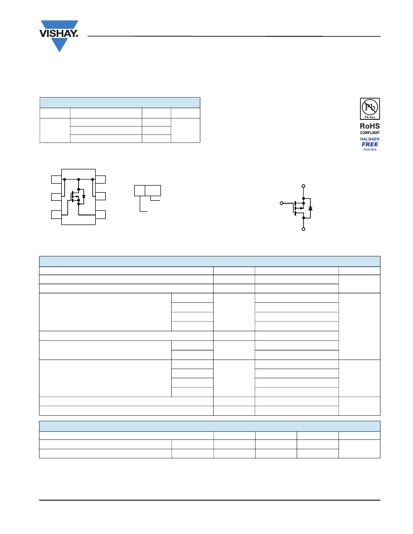
SOT-363
SC-70 (6-LEADS)
? Load Switch for Portable Devices
D
1
6
D
Marking Code
S
BN XX
D
2
5
D
Lot Traceability
and Date Code
G
G
3
4
S
Part #
Code
Top View
Ordering Information: Si1471DH-T1-E3 (Lead (Pb)-free)
Si1471DH-T1-GE3 (Lead (Pb)-free and Halogen-free)
ABSOLUTE MAXIMUM RATINGS T A = 25 °C, unless otherwise noted
D
P-Channel MOSFET
Parameter
Drain-Source Voltage
Gate-Source Voltage
T C = 25 °C
Symbol
V DS
V GS
Limit
- 30
± 12
- 2.7 c
Unit
V
Continuous Drain Current (T J = 150 °C) a, b
Pulsed Drain Current (10 μs Pulse Width)
Continuous Source-Drain Diode Current a, b
T C = 70 °C
T A = 25 °C
T A = 70 °C
T C = 25 °C
T A = 25 °C
T C = 25 °C
I D
I DM
I S
- 2.7 c
- 2.8 a, b
- 2.3 a, b
-8
- 2.3
- 1.25 a, b
2.78
A
Maximum Power Dissipation a, b
T C = 70 °C
T A = 25 °C
P D
1.78
1.5 a, b
W
T A = 70 °C
1 a, b
Operating Junction and Storage Temperature Range
Soldering Recommendations (Peak Temperature) c, d
T J , T stg
- 55 to 150
260
°C
THERMAL RESISTANCE RATINGS
Parameter
Symbol
Typical
Maximum
Unit
Maximum Junction-to-Ambient a, d
Maximum Junction-to-Foot (Drain)
t ≤ 5s
Steady State
R thJA
R thJF
60
34
80
45
°C/W
Notes:
a. Surface mounted on 1" x 1" FR4 board.
b. t = 5 s.
c. Package limited.
d. Maximum under steady state conditions is 125 °C/W.
Document Number: 74468
S10-0646-Rev. C, 22-Mar-10
www.vishay.com
1
发布紧急采购,3分钟左右您将得到回复。
相关PDF资料
SI1557DH-T1-E3
MOSFET N/P-CH 12V SC70-6
SI1563EDH-T1-GE3
MOSFET N/P-CH 20V SC70-6
SI1900DL-T1-E3
MOSFET N-CH DUAL 30V SC70-6
SI1902DL-T1-GE3
MOSFET N-CH G-S 20V DUAL SC-70-6
SI1926DL-T1-E3
MOSF N CH DUAL D-S 60V SC-70-6
SI1967DH-T1-E3
MOSFET 2P-CH 20V 1.3A SC70-6
SI1970DH-T1-GE3
MOSFET N-CH DUAL 30V SC70-6
SI2300DS-T1-GE3
MOSFET N-CH 30V SOT-23
相关代理商/技术参数
SI1472DH
制造商:VISHAY 制造商全称:Vishay Siliconix 功能描述:N-Channel 30-V (D-S) MOSFET
SI1472DH-T1-E3
功能描述:MOSFET 30V 5.6A 2.8W 57mohm @ 10V RoHS:否 制造商:STMicroelectronics 晶体管极性:N-Channel 汲极/源极击穿电压:650 V 闸/源击穿电压:25 V 漏极连续电流:130 A 电阻汲极/源极 RDS(导通):0.014 Ohms 配置:Single 最大工作温度: 安装风格:Through Hole 封装 / 箱体:Max247 封装:Tube
SI1473DH
制造商:VISHAY 制造商全称:Vishay Siliconix 功能描述:P-Channel 30-V (D-S) MOSFET
SI1473DH_08
制造商:VISHAY 制造商全称:Vishay Siliconix 功能描述:P-Channel 30-V (D-S) MOSFET
SI1473DH-T1-E3
功能描述:MOSFET 30V 2.7A 2.78W 100 mohms @ 10V RoHS:否 制造商:STMicroelectronics 晶体管极性:N-Channel 汲极/源极击穿电压:650 V 闸/源击穿电压:25 V 漏极连续电流:130 A 电阻汲极/源极 RDS(导通):0.014 Ohms 配置:Single 最大工作温度: 安装风格:Through Hole 封装 / 箱体:Max247 封装:Tube
SI1473DH-T1-GE3
功能描述:MOSFET 30V 2.7A P-CH MOSFET RoHS:否 制造商:STMicroelectronics 晶体管极性:N-Channel 汲极/源极击穿电压:650 V 闸/源击穿电压:25 V 漏极连续电流:130 A 电阻汲极/源极 RDS(导通):0.014 Ohms 配置:Single 最大工作温度: 安装风格:Through Hole 封装 / 箱体:Max247 封装:Tube
SI1480DH-T1-GE3
功能描述:MOSFET 100V 200mOhm@10V 2.3A N-Ch
RoHS:否 制造商:STMicroelectronics 晶体管极性:N-Channel 汲极/源极击穿电压:650 V 闸/源击穿电压:25 V 漏极连续电流:130 A 电阻汲极/源极 RDS(导通):0.014 Ohms 配置:Single 最大工作温度: 安装风格:Through Hole 封装 / 箱体:Max247 封装:Tube
SI1488DH
制造商:VISHAY 制造商全称:Vishay Siliconix 功能描述:N-Channel 20-V (D-S) MOSFET
